
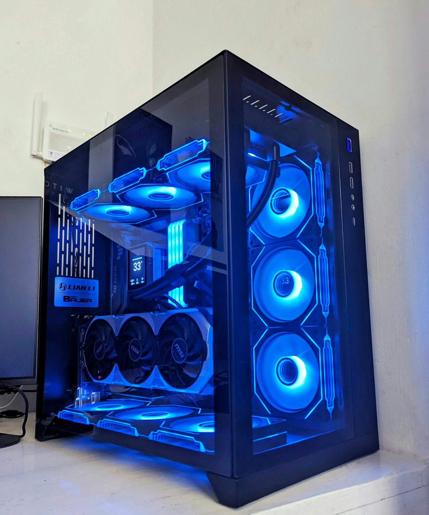
It looks that the race among hyperscalers to replace NVIDIA GPU’s is accelerating whyle simultanusly they’re securing purchase agreements with NVIDIA and AMD . Faced with this apparent contradiction, I’ll try to find some answers.
What is an ASIC?
An ASIC (Application-Specific Integrated Circuit) is an integrated circuit designed to optimally execute a limited set of computational functions, in contrast to general-purpose architectures such as those found in CPUs or GPUs.
Let’s start with the architecture. In a general-purpose processor, the hardware is built to support a wide range of instructions and execution patterns: complex control flow, irregular memory access, multitasking. That flexibility entails inevitable trade-offs: control logic, more general memory hierarchies, less specialized pipelines. In short, in general-purpose architectures there are:
- Complex control logic (branch prediction, instruction scheduling, out-of-order execution)
- Support for multiple instruction types
- Handling of irregular control flow
- Hierarchical caches for unpredictable memory access
An ASIC eliminates or drastically reduces these layers because it operates on the premise that the computation pattern is already known, redirecting the overhead toward compute units (explicit data flow and local data reuse) since it assumes that the original “general-purpuse” overhead will not be necessary.
Instead, ASICs redirect these resources toward three specific things:
- Computing density
- Explicit data flow mapped directly to the hardware.
- Maximize data reuse to avoid frequent access to DRAM.
- Try to adapt the model to the hardware, not the other way around.
A systemic problem in modern computing is the cost of data movement. A GPU is not structurally optimized for this; it attempts to mitigate the issue but does not eliminate it. As Vivienne Sze proposes in her paper:
DRAM accesses require up to several orders of magnitude higher energy than computation
This directly affects architectures such as those of GPUs, which rely on memory hierarchy to support their parallelism.
Moving data is expensive, so an ideal system is one in which data movement is minimized; ASICs come close to this, but there are other options.
Efficiency depends on maximizing data reuse and minimizing DRAM accesses. While GPUs attempt to approximate this principle through caches and memory hierarchies, ASICs incorporate it directly into their architecture, organizing computations so that data is reused locally and frequent accesses to external memory are avoided.
“the 3000M DRAM accesses in AlexNet can be reduced to only 61M”
The ASIC, therefore, redesigns the computational flow to bypass the most expensive component of the system.
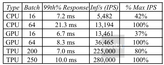
This approach yielded measurable results. In the seminal paper by Jouppi et al. (ISCA 2017), Google reports significant improvements in inferences per second compared to the GPU.
The TPU die is now 15.3 times as fast as the GPU die
The results were consistent; even though they come from the V1 version, they give us an idea of the direction Google has taken in designing its chip architecture.
An ASIC, therefore, should not be viewed as a more efficient version of a general-purpose processor, but rather as a different architectural approach in which flexibility is sacrificed in order to optimize performance around a dominant pattern.
How are the hyperscalers’ efforts to build their own chips coming along?
During its latest earnings call, Meta announced a capital expenditure budget of between $115 billion and $135 billion for 2026. This represents an increase of more than 90% compared to 2025.
During the fourth-quarter 2025 results conference call, Mark Zuckerberg said:
An important part of Meta Compute will be making long term investments in silicon and energy [ …] We’re architecting our systems so that we can be flexible in the systems that we use and we expect the cost per gigawatt to decrease significantly over time through optimizing both our technology and supply chain.
Meanwhile, Microsoft closed Q2 of FY2026 with $22.6 billion in quarterly capital expenditures.
Google and Amazon are also engaged in a race to spend on infrastructure.
The combined capex projection for 2026 which comes from their guidelines will growth almost 70%
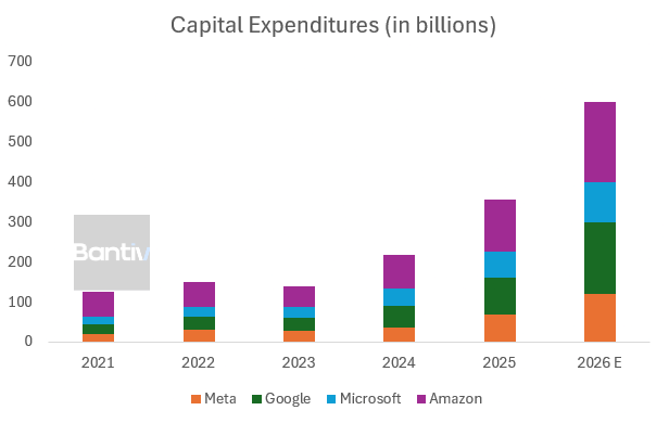
This raises the question: if you’re buying hundreds of thousands of NVIDIA H100 and B200 GPUs, why bother designing and building your own chip?
Here is what Satya Nadella said during the Q2 FY2026 earnings call:
We want a fleet at any given point in time to have access to the best TCO… because we can vertically integrate doesn’t mean we just only vertically integrate.
It is building a heterogeneous fleet where Maia 200, Blackwell, and AMD MI300X coexist, and where workload allocation decisions are optimized in real time based on total cost of operation.
Meta is doing the same. During its Q1 2026 earnings call, the company confirmed that its Andromeda ad retrieval engine runs simultaneously on NVIDIA, AMD, and MTIA.
The pivot to training
Initially, ASICs were primarily designed for inference.
However, it seems they want to move to training too, just like Meta says in a Q4 2025 earning call :
“In Q1, we will extend our MTIA program to support our core ranking and recommendation training workloads, in addition to the inference workloads it currently runs.
An inference workload has a well-defined form and stable architecture. It is exactly the type of problem for which an ASIC can outperform a GPU in terms of energy efficiency and cost per operation.
Meta is executing this plan with precision. In Q1 2026, it confirmed that MTIA, its Meta Training & Inference Accelerator, is running production inference workloads. And it goes even further:
In Q1, we will extend our MTIA program to support our core ranking and recommendation training workloads.
This is clearly shows Meta’s intention not only to remain in inference, but also intervene NVIDIA’s lock-in for training. They are starting with recommendation workloads that are computationally more predictable .
In 2026, Meta unveiled four in-house chips designed for AI tasks. The MTIA300 is the latest iteration, which is currently in production deployment. In fact, Meta has been building this capability in-house for multiple generations, meaning the program has been maturing for years,
To build a chip
Manufacturing a chip isn’t cheap; it requires phases, long-term coordinations and its capital intensive and build partnerships across the value chain. time.
Even so, once a version has been built, pivoting also comes at a cost.
Broadcom comes into play on the design side. The company is the go-to design partner for multiple hyperscalers in their ASIC programs, particularly in networking, I/O, and system-level integration. Google’s TPU chip project, and several others rely on Broadcom for interconnect and packaging design. Marvell holds a similar position.
The obvious risk for Broadcom is what happens when the customer internalize these capabilities? Is it possible that once Google has internalized enough know-how, it could do without its design partners?
The short answer is that it is unlikely, though that risk will always exist. Chip designers at the hyperscaler scale remains a field of coordination where Broadcom and Marvell’s expertise in IP blocks, packaging, interconnect its difficult to replace and absorving this capacity is slow .
The real issue
There is currently a bottleneck that all manufacturers (in-house or external) face: High Bandwidth Memory.
Micron is straightforward in its Q1 FY2026 earnings report:
HBM supply is sold out for multiple years.
The company projects a TAM CAGR of approximately 40% for HBM through 2028, from ~$35 billion in 2025 to ~$100 billion in 2028, and is raising its fiscal 2026 capital expenditures to $20 billion (from the previously estimated $18 billion) to expand HBM capacity.
First, the HBM shortage affects both NVIDIA and the hyperscalers equally. The Blackwell B200 requires HBM3e. Next-generation ASICs do as well.
Second, the HBM market is typically cyclical and has high barriers to entry. SK Hynix, Samsung, and Micron are the only major players. As a result, chip developers will seek to secure their supply contracts.
Meta may design the MTIA300, but it still needs HBM. This indirectly supports demand for NVIDIA GPUs, which already have established supply contracts.
SK Hynix confirmed that its entire DRAM, NAND, and HBM production is sold out through the end of 2026, largely committed to NVIDIA for its AI accelerators.
Conclusion
Hyperscalers seem to be aiming to verticalize and dominate the platforms on which they develop their products. Chips are no exception.
However, the fact that hyperscalers manufacture their own chips in-house does not change the fact that they rely on the supply chain and suppliers.
Ultimately, hyperscalers remain dependent on external foundries such as TSMC for fabrication, HMB suppliers and so on, reinforcing the interdependence across the semiconductor stack.